Frequency Domain Relationships and Compensation
Leave a reply
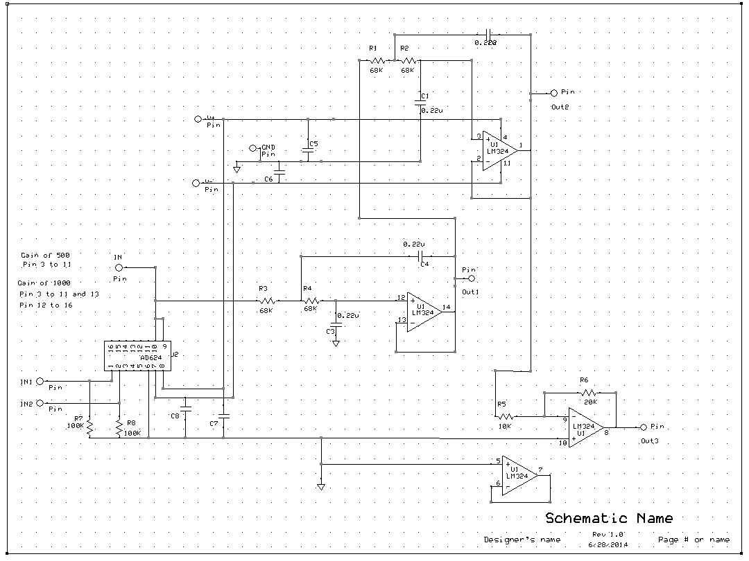
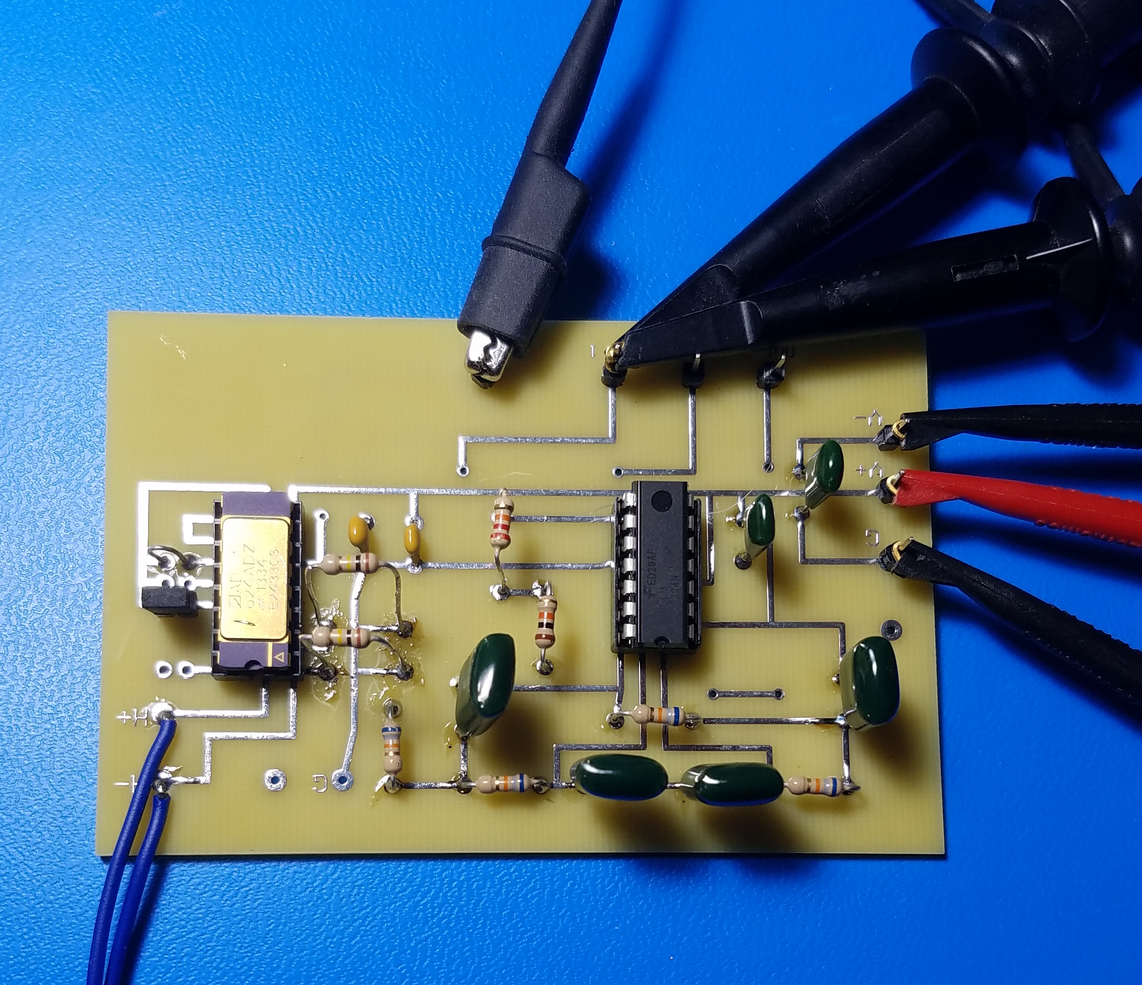
This is a simple design of a two-lead EKG amplifier. The real work is done by the AD624 inamp. In order to get rid of 60Hz, the amplifier is followed by two Sallen-Key low-pass filters. It turns out that only the first one is necessary. The second one reduces the rise and fall time of the QRS pulse.
The trickiest part of making this work is the leads. By just holding the leads with left and right hand, there is a lot of baseline wander. Best result is obtained using actual EKG sense pads.
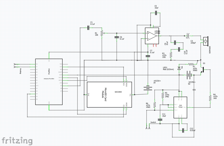
This project uses an Arduino Pro Mini, SD card reader, LM386 audio amplifier, and a 555 timer.
A list of short phrases are stored on the SD card. When a button is pushed, the Arduino powers up and randomly plays one of the stored phrases. Then it powers down. The 555 controls the timing for powering the Arduino. By using the 555, the overall system uses much less power since it is only powered for about 10 or so seconds (choosing different timing components will achieve different power-on times).
The wav file is played using the TMRpcm Arduino library. In order to play a wav file, it must have the following characteristics:
Name: maximum of 8 characters with no extension
Samples per second: 16000
Channel: Mono
Bits per sample: 8
Using Audacity, any wav file can be reformatted to these settings.
Schematic:
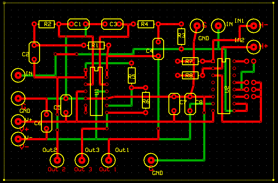
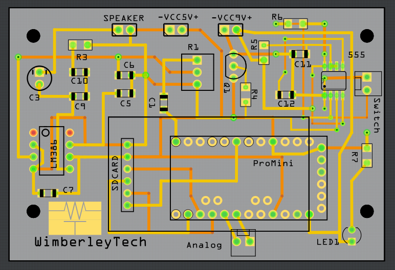
Board Layout:
Fritzing file with code:
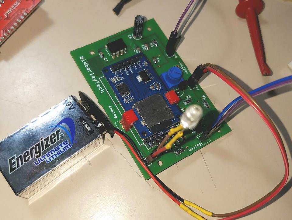
Here is the finished product!
Here is an outline of the setup process. These instructions assume that the device is in default mode from factory and never been programmed.
Plug the USB into the Arduino and load a blank Sketch using the keyboard shortcut: CTRL+N. It should look like Figure 1.
Disconnect power to the Arduino. Connect RX and TX pins as shown in Figure 1. Note that RX goes to RX (with voltage divider) and TX to TX. This is the required connection for AT command mode.
 Figure 1
Physically mark the slave device with an “S” with a marker so that you will not lose track of which is the slave device. We will do the same with the master in a later step.

Figure 2
Apply power to the Arduino by plugging in the USB. The LED on the HC-05 should blink at 2-second intervals. (Some instructions tell you to press the small button on the HC-05 while applying power. However, it is not necessary if EN (Key) is hard-wired to 3.3V. The button on the HC-05 is useful, as it can be used as an alternative to hard-wiring EN (Key) pin to 3.3V. Simply leave EN (Key) pin disconnected and hold the button while powering the Arduino. )
Next, the Slave will be setup using AT commands. Open a terminal window in the Arduino environment (CTRL+SHIFT+M). Set baud rate to 38400 if it is not already. Set “Both NL and CR” at the bottom of the terminal window.
Start first AT commands by typing:
AT
The response should be “OK” or sometimes “ERROR(0)” but ignore the latter, just type AT again to get the “OK” response.
Confirm that the device being set up as a Slave, type
AT+ROLE?
The response in the terminal window should be:
+ROLE:0
This indicates “Slave” mode. If instead the device was previously setup as a Master, we would not to change ROLE to 1. Setting ROLE to 1 will be described in the Master Setup section of this tutorial.
Next get the address of this HC-05 module.
AT+ADDR?
The HC-05 will respond with a number that looks similar to this: 98d2:31:fd4ea1 This number must be recorded on paper or in a notepad on your computer. It will be needed later.
This is all that is required for the Slave module.
Unplug the Arduino.
Plug the USB into the Arduino and load a blank Sketch in the Arduino environment using the keyboard shortcut: CTRL+N. It should look like Figure 1.
Initial wiring for Master setup is the same as it was for Slave setup and is shown in Figure 2. Physically mark the slave device with a “M” with a marker so that you will not lose track of which is the slave device.
Apply power to the Arduino by plugging in the USB. The LED on the HC-05 should blink at 2-second intervals. (Some instructions tell you to press the small button on the HC-05 while applying power. However, it is not necessary if EN (Key) is hard-wired to 3.3V. The button on the HC-05 is useful, as it can be used as an alternative to hard-wiring EN (Key) pin to 3.3V. Simply leave EN (Key) pin disconnected and hold the button while powering the Arduino. )
Next, the Master will be setup using AT commands. Open a terminal window in the Arduino environment (CTRL+SHIFT+M). Set baud rate to 38400 if it is not already. Set “Both NL and CR” at the bottom of the terminal window.
Three things must be accomplished setting up the Master module
Start first AT commands by typing:
AT
The response should be “OK” or sometimes “ERROR(0)” but ignore the latter, just type AT again to get the “OK” response.
Change the ROLE of the device to Master, type
AT+ROLE=1
The response in the terminal window should be:
OK
Verify that the change was made by typing:
AT+ROLE?
The response should be:
+ROLE:1
Next, check the connection mode:
AT+CMODE?
The device will probably return:
+CMODE:1
This means that the device can connect to any device. Change it to CMODE=0 because we want to talk to only one device.
AT+CMODE=0
The response should be “OK”
Next bind address of this HC-05 module to the Slave device using the Slave address captured earlier. However, we will replace the colons (“:”) with commas (“,”).
AT+BIND=98d2,31,fd4ea1
The HC-05 will respond with “OK”
This is all that is required for the Master module.
Now that Master and Slave modules have been setup, the wiring must be changed in order for them to communicate. The wiring change is identical for Master and Slave and is described below.
Disconnect power. Remove the connection between EN (Key) and 3.3V, and switch RX and TX connections at the Arduino resulting in the circuit shown in Figure 3. Make these changes on both devices.
Power both devices. After a few moments, both devices should be blinking quick blinks in close synchronicity about every two seconds.
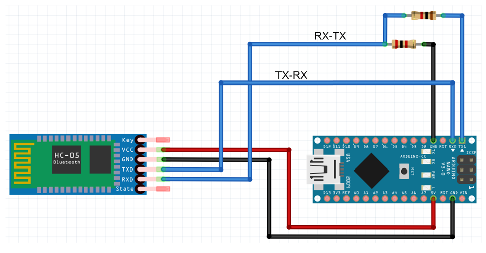
Figure 3
Next, step is writing application code to send information between master and slave. Simple enough, but the HC-05 attached to the RX/TX pins impedes downloading code to the Arduino. So, in order to download code, the RX and TX pins need to be temporarily removed. After download, they may be re-attached. For a final product, a DPDT switch can be installed inline with the RX/TX pins.
Credits
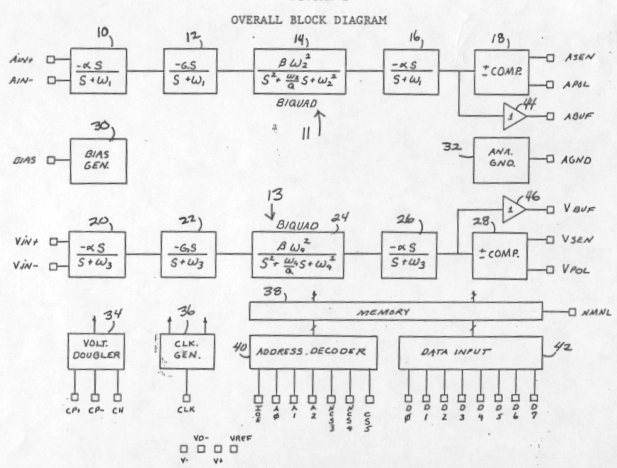
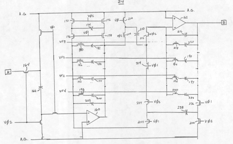
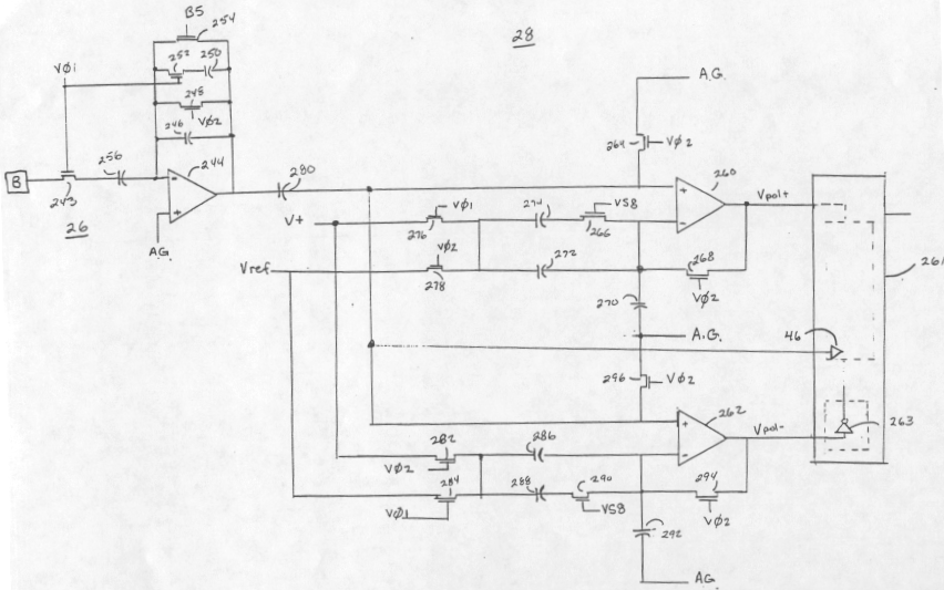
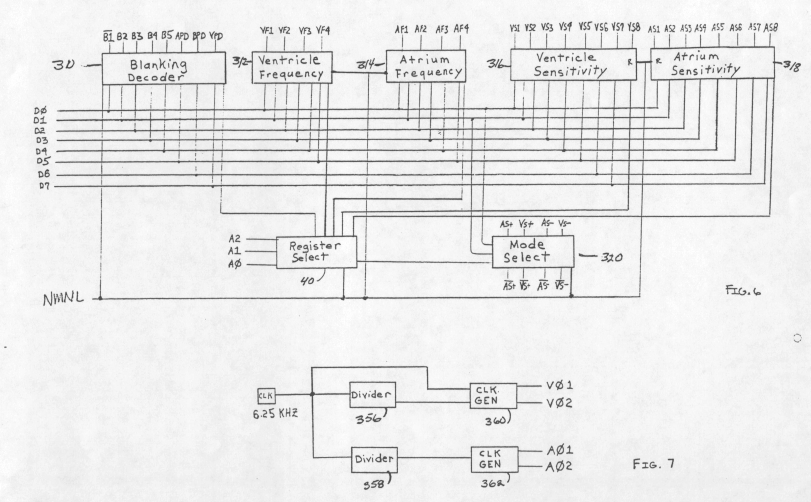
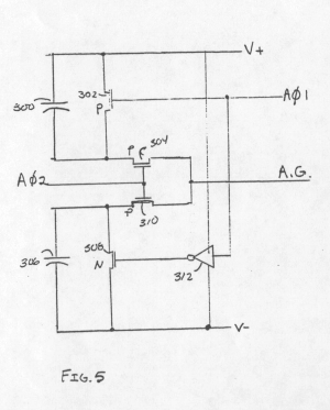
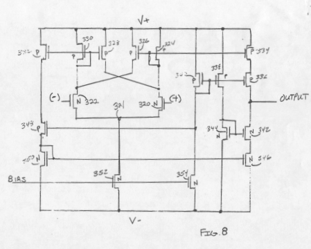
Around roughly 1982, I was contracted to design a sense amplifier/filter as a front end for a heart pacemaker. The specifications were as follows:
Sensitivity: 600uV to 4.2mV — adjustable
S/N: 40dB
Filter: Programmable 5-poles, three zeros, nominal 30Hz center and 45Hz BW.
Supply: 2.0-3.3 V with maximum 4.5uA current
The circuit was designed in 5uM Si-Gate CMOS P-well process.
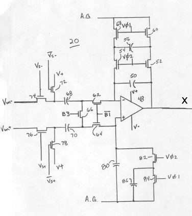
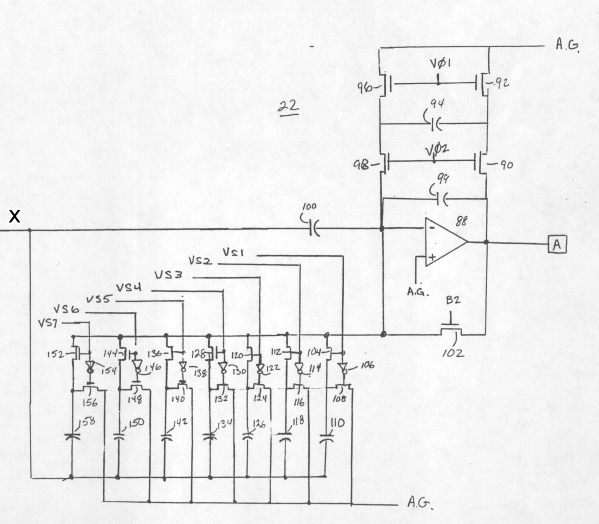
I am pretty sure this was the first switched-capacitor implementation of a pacemaker sensing channel. The simplified schematics are shown below.
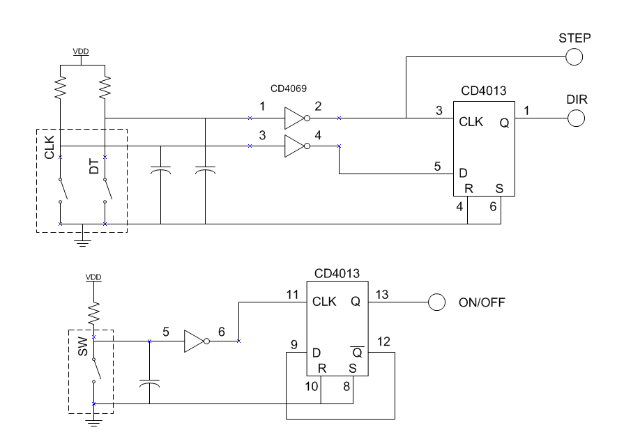
I bought some rotary encoders to interface with an Arduino. There are examples of code that can be used to read the encoder in a variety of websites. The one I tried was a little glitchy, but it may be due to not doing any filtering of the switch outputs. So, I was going to add some caps and clean up the outputs but decided that I would rather implement the decoding function in hardware. This would simplify the code and use fewer Arduino resources.
Decoding a rotary encoder is very simple with just a D-Flip Flop. One encoder switch output goes to D and the other goes to CLK. I figured that I was not the only person to arrive at this realization. Sure enough, I found a very nice writeup on an implementation using a DFF here: http://AC-DC Switching regulator uninterruptible power supply.
The addition of the Schmitt triggers is a nice touch for additional noise immunity. Not having any, I decided to build the circuit using a CD4069 hex inverter. I also wanted to incorporate the push switch feature of my rotary encoder, so my design is a little different.
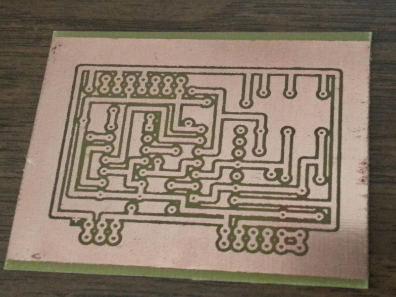
During the same time I was thinking about rotary encoders, I was also pondering DIY PC boards. This was the perfect project for that. After lots of back and forth, I decided on using the hot-toner-transfer method. I ran a number of experiments to perfect the method and arrived at the following very simple methodology.
I have made several board. For one, I heated the Ferric Chloride with a hot plate. The etch went very fast. The second time I did not heat the fluid and the etch took longer.
Here is the resulting PCB
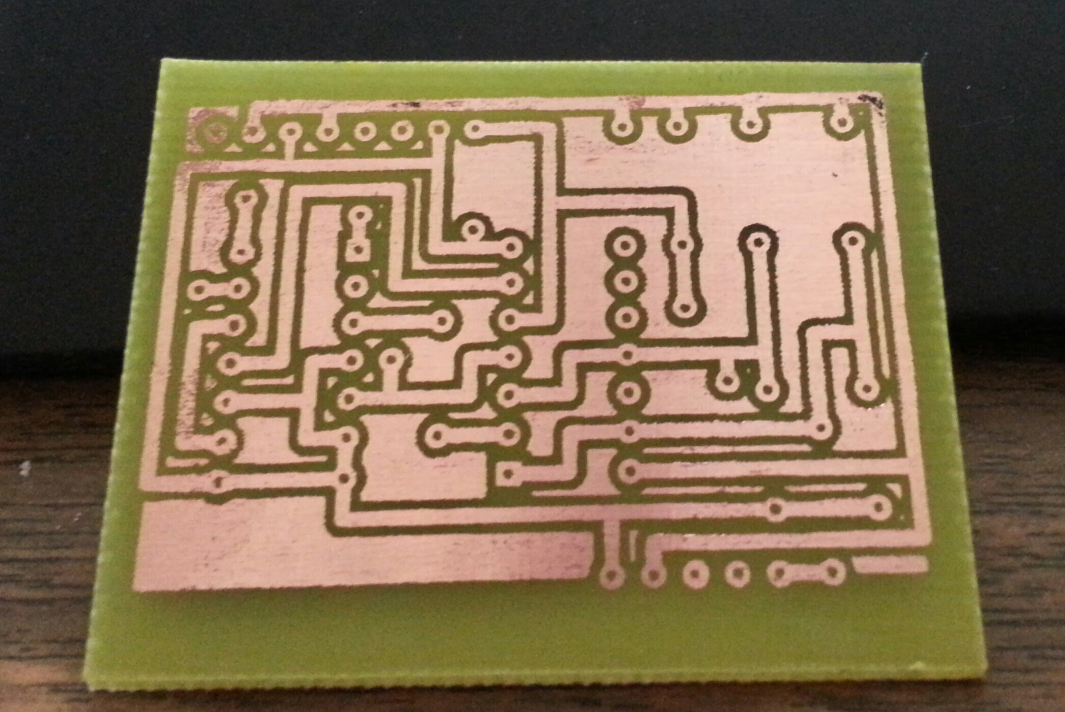
It is not perfect, but not bad for very early in the learning curve! The key to successful etching is adding the flood fill so that etching can be uniform (more or less) throughout.
I populated the board as shown below
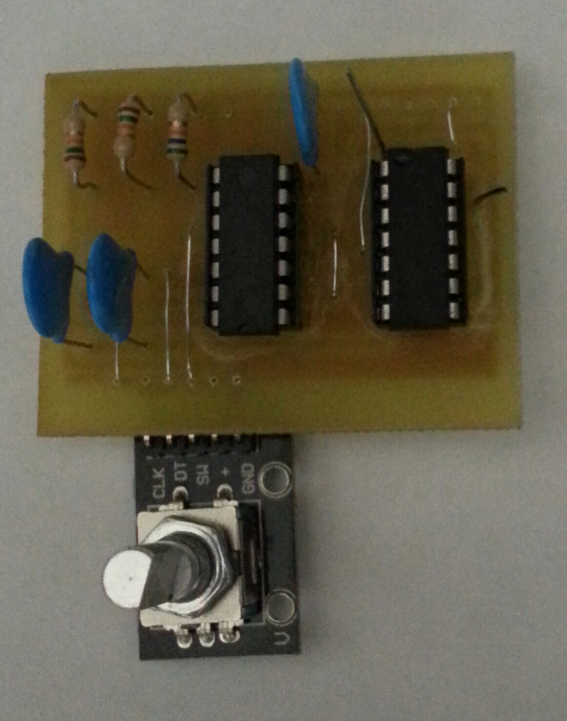
The caps are 22nF and the resistors are 15K. Not critical.
I powered it up and it worked just fine!!
A few days later I decided to improve the layout so that I can attached the rotary encoder with a stake header. Also, I wanted another iteration of my lithography and etching technique. Here is the updated board. Quite nice.
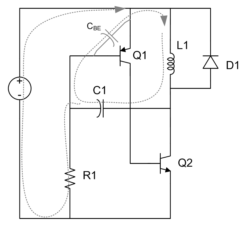
I saw this circuit on a Youtube EEVBlog video. It is an LC relaxation oscillator. I do not recall seeing a relaxation oscillator using inductors and capacitors, so naturally it piqued my interest. Here is the circuit.
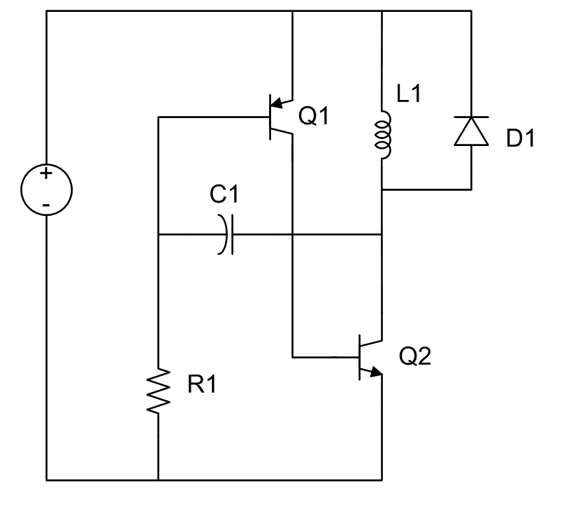
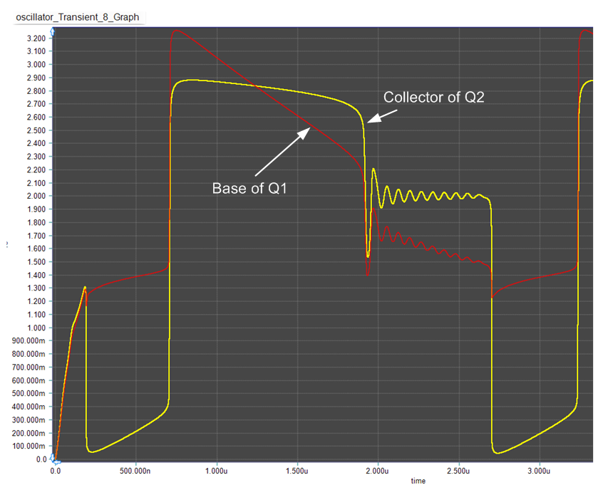
The first thing I did was build the circuit in the lab and see how it performed. I used an LED for the diode.
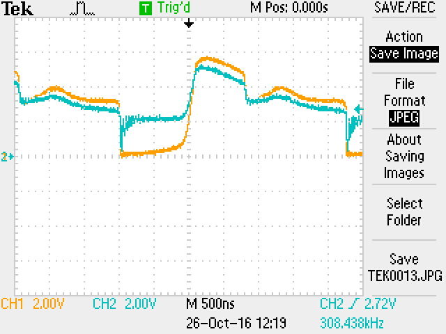
Yellow is the collector of Q2 and the blue is the base of Q1.
Very interesting waveshape. Let’s see how this circuit works.
When power is applied, Q1 and Q2 turn on. Collector of Q2 pulls to ground. Since current cannot change instantaneously, the voltage applied across the inductor allows a fixed di/dt to charge the inductor, L1. The current starts flowing in a roughly linear fashion until the maximum current that can be supplied by Q2 is reached…at which time di/dt falls to zero.
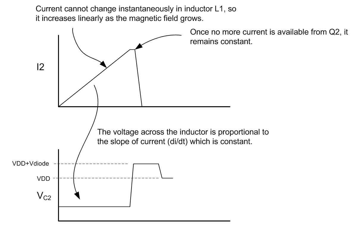
When Q2 current saturates, di/dt=0 and the inductor cannot maintain the voltage across it so the collector of Q2 swings positive. This voltage couples to the base of Q1 to turn it off (positive feedback) and thereby cutting off the Q2 collector current to the inductor which tries to maintain its magnetic field and propels even more positive until it discharges through the diode.
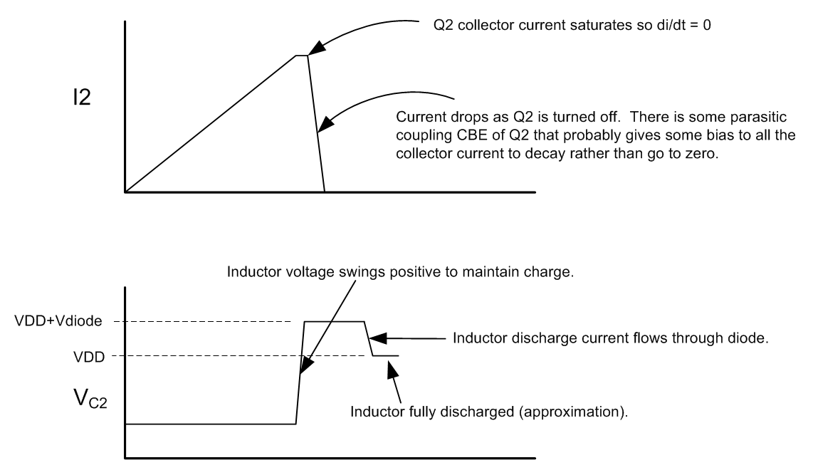
Inductor discharge current flows through diode until the voltage collapses across the inductor. The time in this state is determined by the R1*C1 time constant. By modifying this time constant, this pedestal can be lengthened or shortened.
The inductor cannot completely discharge through the diode because of the diode junction voltage requirement. The inductor must finish discharging via parasitic paths in the circuit. The only path for discharge is through C1 and CBE in parallel with R1 as shown below.
The inductor discharges via the parasitic path until the base of Q1 discharges enough to turn on Q1 and repeat the cycle.
A simulation of the circuit illustrates the phases of operation.
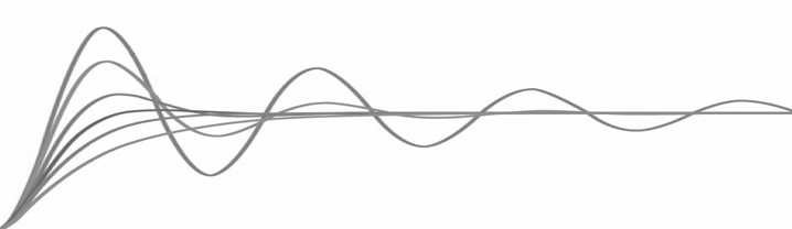
If the RC time constant is chosen short enough, the portion of the waveform that is ringing can be eliminated.
OK…interesting circuit. Quite complicated due to the inductor. It does oscillate. But why would you build such a circuit. Well, perhaps for the LED drive. Typically, and LED may require a forward voltage of 1.8 to 2.8 volts. If you wanted to power the oscillator with a single cell, then maybe you need the inductor kick-back voltage for that.
I presented this in 1998. How much of it is still true?
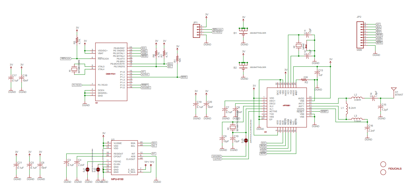
A client asked me to develop a multi-axis sensor for embedded applications. It needed a gyro, accellerometer, and a magnetometer, so I decided on the Invensis 9150 9-axis motion sensor. In order to output the data to something, I used Bluetooth LE so that I could communicate with a smart phone (Android or IOS). At the time, the most popular BTLE device seemed to be the Nordic nRF8001. For control, I could have gone several ways. There was a lot of code in the public domain using Arduino which is based on Atmel AVR devices primarily. However, due to my roots, I decided on the Silicon Labs C8051F931. The circuit design was easy. Most of the work had already been done by others in terms of the radio…the rest was just connecting pins! Here is the schematic.
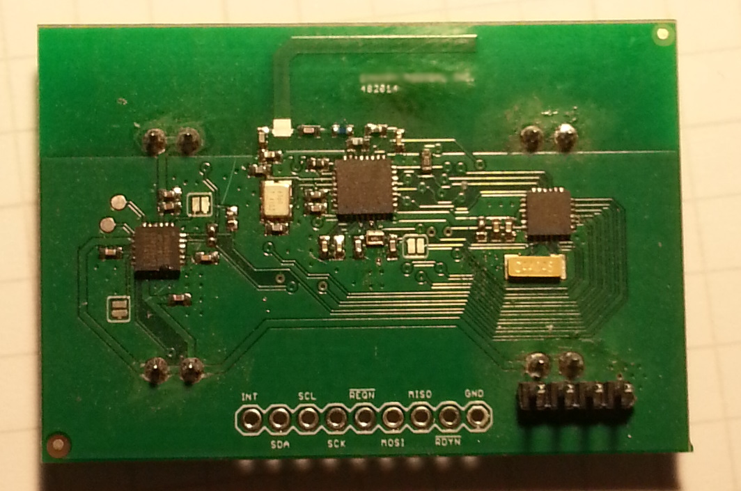
Next task was to do the board layout. I have a guy that is good at this sort of thing, so I contracted it out…both board design and assembly. Here is the result.
Once the schematic was done, I set about writing the code. I started with the codebase that was developed for the Arduino. Basically, I had to port everything over to the Silabs MCU. It was not trivial, but after some effort, I got it working.
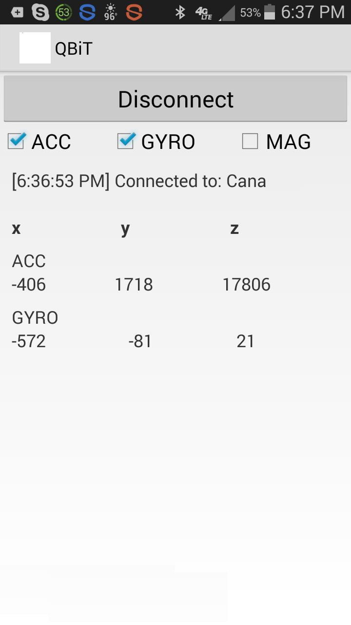
I also benefited from the work Nordic and others had done on the smartphone side. So I had my son take the Arduino Android code and modify it to interface with my board. Here is a screen shot of an Android phone showing the results being read from the board over BTLE.
This was a great project!!