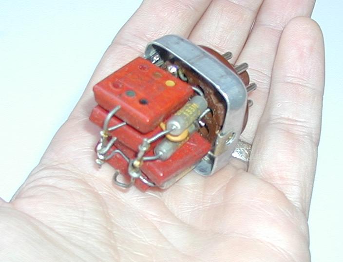
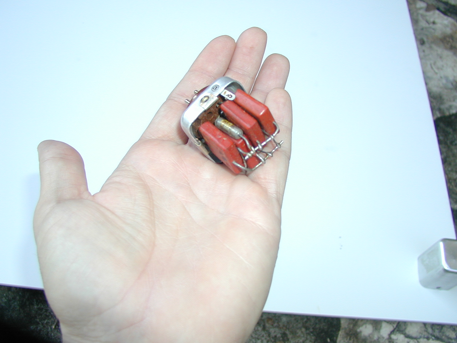
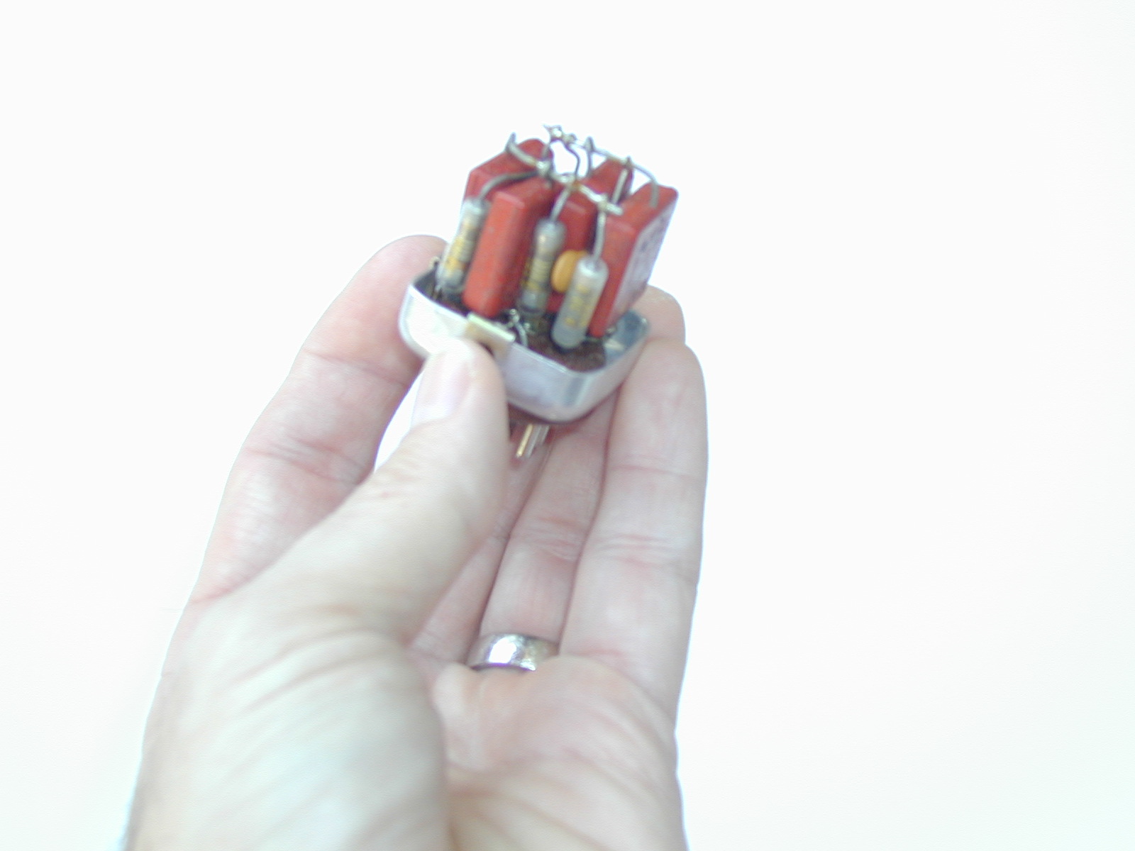
Over the years, a lot of things have changed in the lab. VOMs have given way to the DMM, analog spectrum analyzers have been replaced by FFT engines, analog storage oscilloscopes have yielded to digital storage scopes—in fact analog scopes sans storage have been virtually replaced by digital ones (my Tek 465 is the mainstay in my lab at home). And finally, knobs have been punched out by arrays of buttons! Yet the 10X scope probe has remained fairly constant through the many other technological advances. Scope probes are interesting.
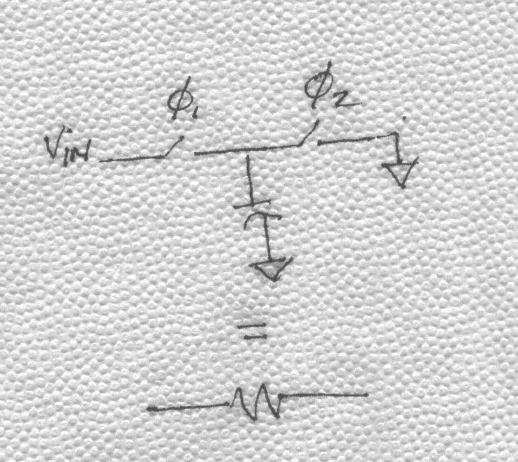
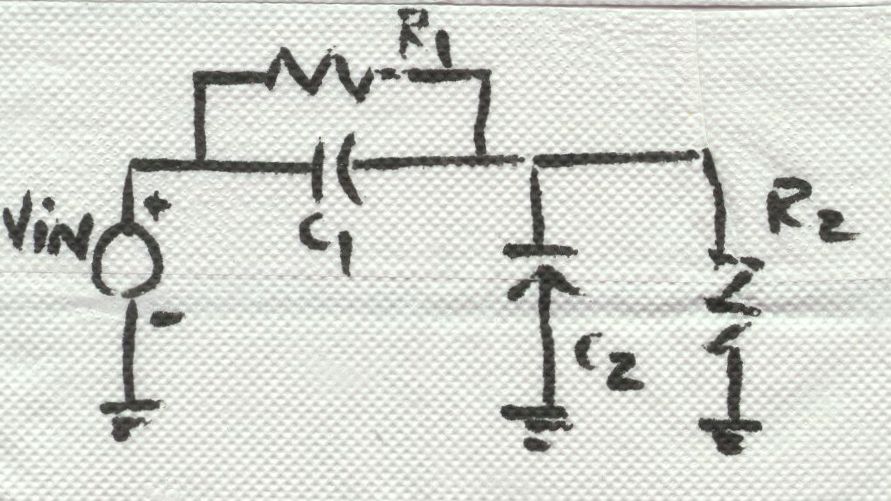
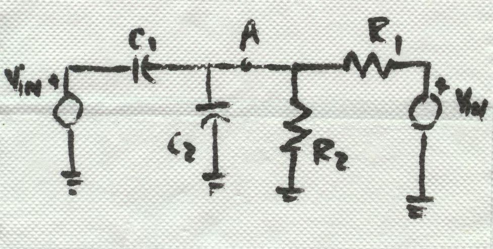
A simplified drawing of a scope-probe network is illustrated in BarNapkin 1.
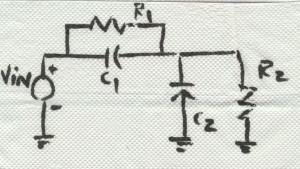
BarNapkin 1
By observation, you can see that the network has one pole and one zero. In a typical scope probe, a portion of capacitor C2 and resistor R2 are present at the input of the scope itself. Capacitor C1 and resistor R1 are built into the probe and C1 is tunable. As the instruction manual guides, you are to apply a square wave to vin and adjust the capacitor until a square wave is observed on oscilloscope screen. What is this adjustment doing? The presence of C1 creates a zero in the transmission path. A pole also exists and is due to all of the capacitance connected at the junction of C1 and C2. The adjustment moves the zero so that it lies on top of the pole thus canceling the effect of both and achieving an infinite bandwidth transmission path! (We all know you don’t get infinite bandwidth and the reason is because there are other parasitics not accounted for in this simple equivalent model.) This pole-zero pair that you are aligning by adjusting C1 is referred to as a pole-zero doublet.
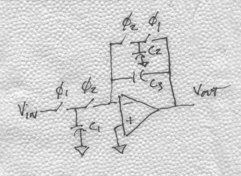
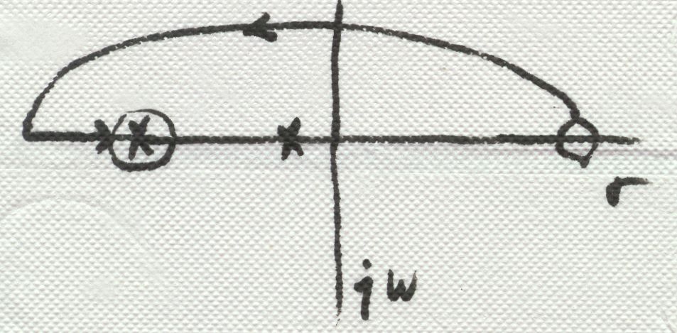
Analog CMOS circuit designers come across pole-zero doublets when trying to maximize bandwidth of a two-stage operational amplifier without sacrificing stability or settling time. The doublet occurs when the you try to move the naturally-occurring right-half-plane zero (due to Miller compensation) into the left-half plane on top of the amplifier’s output load-determined pole as illustrated on BarNapkin 2.
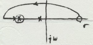
BarNapkin 2
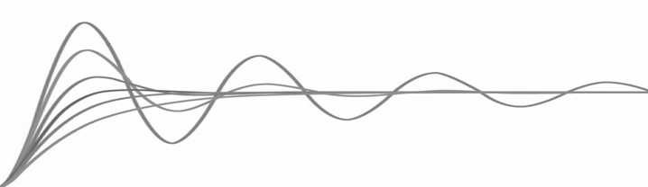
You can never get it exactly right. You might think a Bode plot including the effect of the doublet would give you comfort. Well, it doesn’t–they are close together but you just can’t see their effect in the frequency domain. However, it is well known that such doublets cause a deterioration of the time-domain response of the network in which they lie. Such an effect is often observed to as a “long tail” in the settling response. How can this be? Well, if you do the analysis in the time domain (or in the S-domain and dig out your table of Laplace transforms), you will get the answer you are searching for. For the abstract mind, this is good enough—move on. But, if you want some intuitive insight, sit back, and enjoy.
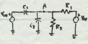
Referring again to BarNapkin 1, the zero comes about from the capacitor C1 acting with R1 yielding a zero at wZ = 1/R1C1 and a pole at wP = 1/(C2+C2)(R1|| R2). Applying a simple network-analysis trick allows us to develop some intuition. Let’s split the input voltage source into two voltage sources—one driving C1 and the other driving R1 as illustrated in BarNapkin 3.
BarNapkin 3
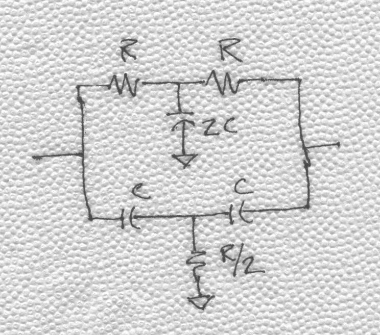
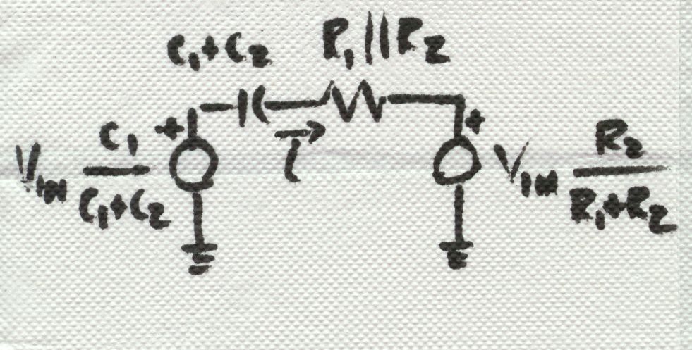
Using Thevenin equivalents looking both ways from node A, we get the equivalent circuit shown on BarNapkin 4.
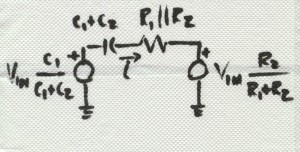
BarNapkin 4
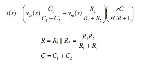
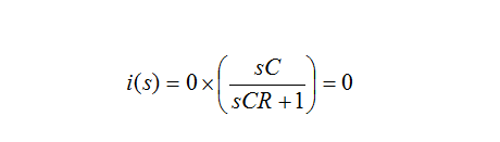
Nothing has changed about the circuit. It has been rearranged to aid intuition. Now, with this rearrangement, it is easy to calculate the current flowing through node A. We can derive the network time constant by examining i(s). We could have stayed in the voltage domain and calculated the voltage across R1 or R2. Either way works since the goal is to determine the response to the stimulus, vin. The current, i(s), through node A is given as:
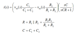
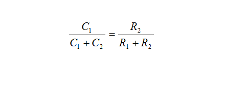
Consider what happens if the two factors of vin are equal as shown in the following expression.
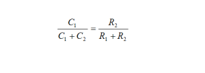
Then
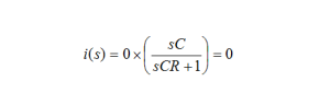
What does zero current mean? It means that there is no displacement current flowing between the resistors and capacitors. Thus, the time constant of this circuit appears to be zero or, said another way, the bandwidth appears to be infinity!
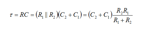
Now, if the two factors of vin are not equal, then the difference forces a current that settles with a time constant of RC as given below

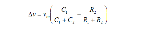
What insight can we glean from these results? Clearly, placing the pole and zero squarely on top of one another achieves the greatest bandwidth. However, if they are not coincident, there appears a time constant, t, which settles a voltage difference of

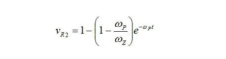
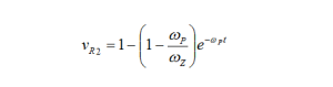
OK, as I said, you could do this analysis in the more classic fashion and arrive at the same understanding (see the expression below for the voltage across R2 resulting from an input step).
However, applying network simplifications such as the Thevenin equivalent allows for quick insight and can often provide the mathematical insight by inspection.