Category Archives: Circuits

EKG Amplifier

This is a simple design of a two-lead EKG amplifier. The real work is done by the AD624 inamp. In order to get rid of 60Hz, the amplifier is followed by two Sallen-Key low-pass filters. It turns out that only the first one is necessary. The second one reduces the rise and fall time of the QRS pulse.

The trickiest part of making this work is the leads.  By just holding the leads with left and right hand, there is a lot of baseline wander.  Best result is obtained using actual EKG sense pads.

Pacemaker Sense Amplifier

Around roughly 1982, I was contracted to design a sense amplifier/filter as a front end for a heart pacemaker.  The specifications were as follows:

Sensitivity: 600uV to 4.2mV — adjustable
S/N: 40dB
Filter: Programmable 5-poles, three zeros, nominal 30Hz center and 45Hz BW.
Supply: 2.0-3.3 V with maximum 4.5uA current

The circuit was designed in 5uM Si-Gate CMOS P-well process.

I am pretty sure this was the first switched-capacitor implementation of a pacemaker sensing channel.  The simplified schematics are shown below.

Rotary Encoder

I bought some rotary encoders to interface with an Arduino.  There are examples of code that can be used to read the encoder in a variety of websites.  The one I tried was a little glitchy, but it may be due to not doing any filtering of the switch outputs.  So, I was going to add some caps and clean up the outputs but decided that I would rather implement the decoding function in hardware.  This would simplify the code and use fewer Arduino resources.

Decoding a rotary encoder is very simple with just a D-Flip Flop.  One encoder switch output goes to D and the other goes to CLK.  I figured that I was not the only person to arrive at this realization.  Sure enough, I found a very nice writeup on an implementation using a DFF here:   http://AC-DC Switching regulator uninterruptible power supply.

The addition of the Schmitt triggers is a nice touch for additional noise immunity.  Not having any, I decided to build the circuit using a CD4069 hex inverter.  I also wanted to incorporate the push switch feature of my rotary encoder, so my design is a little different.

During the same time I was thinking about rotary encoders, I was also pondering DIY PC boards.  This was the perfect project for that.  After lots of back and forth, I decided on using the hot-toner-transfer method.  I ran a number of experiments to perfect the method and arrived at the following very simple methodology.

  1. Design the layout of the board using ExpressPCB software.  Since I am using the toner-transfer method, I will just need to print the resulting layout to a PDF file (I will explain why PDF instead of direct to printer later).  Moreover, I like using ExpressPCB because once I perfect the layout, I can send the design to them and get three double-sided boards for a little over $50.  Since my DIY board is single sided, I laid out the board so that I use minimum of backside traces.
  2. Using Adobe Illustrator (AI), open the PDF file, delete the bounding box that ExpressPCB software generates.  Move the layout to the top of the page, and make a number of copies of the layout and place them in various places on the page.  This gives me the option to do multiple tries as my technique is perfected.  I can also do multiple boards though that is not my goal.  So, the reason for printing to PDF is to give the ability to edit the file in AI.
  3. Print the newly edited PDF file to a real printer.  I have tried the HP LaserJet P1102W using LD Products toner.  Not so good.  Printing to my Brother MFC-7860DW copier/fax/printer generated very nice output.  I printed in 1200 dpi but I don’t think it makes much difference.  I printed to several types of paper (lots of ideas on paper choices can be found on the internet).  I used some transfer paper I bought many many years ago and never used.  It came from DynaArt Designs which is now PulsarProFX.
  4. Transfer the image to a PCB.  Very simple.  Lay the image on a perfectly clean PCB and press a hot iron over it for about three minutes–all the time applying lots of pressure.  The place the board and paper into a water bath and leave it until the paper separates leaving the traces on the PCB.  Takes about another two minutes.
  5. Etch the board using Ferric Chloride.
  6. When etching is complete, rinse in water.  Then remove the traces using acetone.
  7. Done.

I have made several board. For one, I heated the Ferric Chloride with a hot plate.  The etch went very fast.  The second time I did not heat the fluid and the etch took longer.

Here is the resulting PCB

It is not perfect, but not bad for very early in the learning curve!  The key to successful etching is adding the flood fill so that etching can be uniform (more or less) throughout.

I populated the board as shown below

The caps are 22nF and the resistors are 15K.  Not critical.

I powered it up and it worked just fine!!


A few days later I decided to improve the layout so that I can attached the rotary encoder with a stake header.  Also, I wanted another iteration of my lithography and etching technique.  Here is the updated board.  Quite nice.

LC Relaxation Oscillator

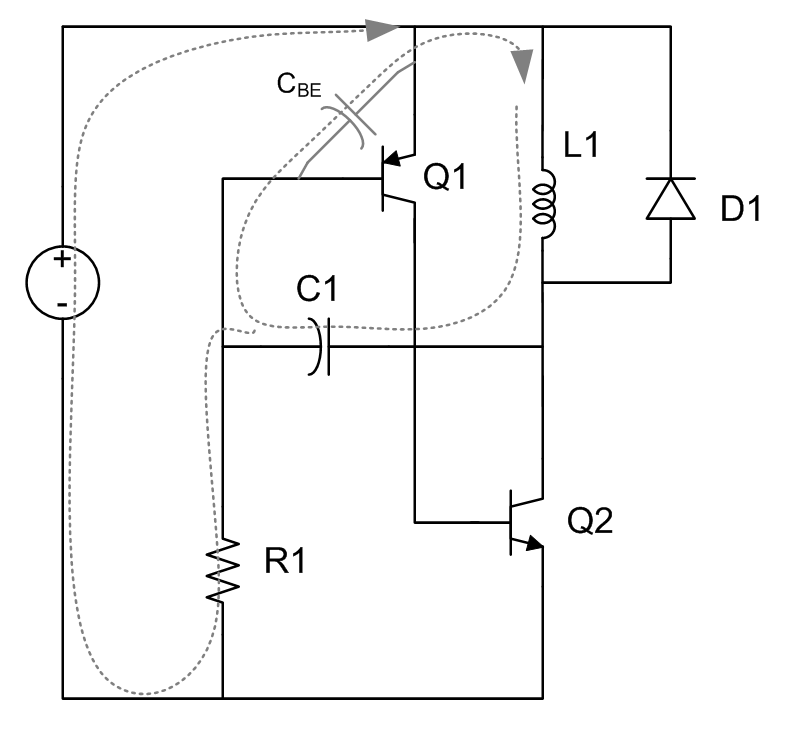
I saw this circuit on a Youtube EEVBlog video.  It is an LC relaxation oscillator.  I do not recall seeing a relaxation oscillator using inductors and capacitors, so naturally it piqued my interest.  Here is the circuit.

lcoscillator

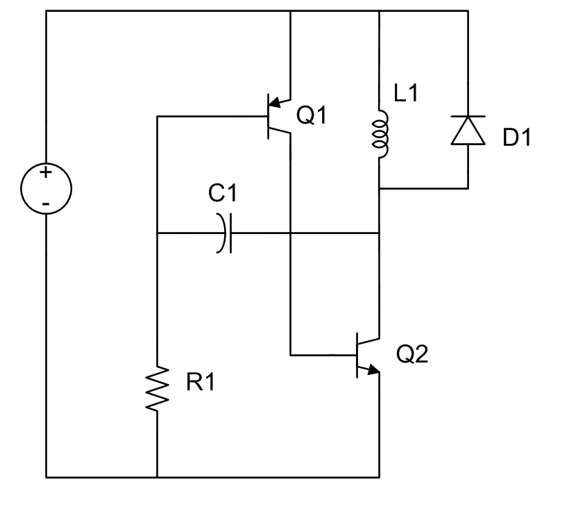
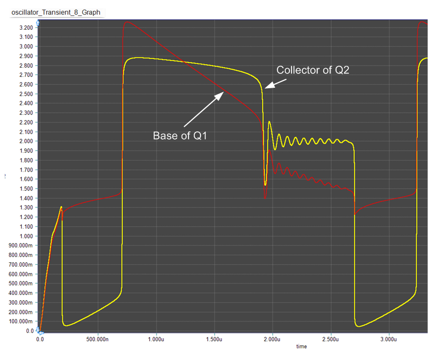
The first thing I did was build the circuit in the lab and see how it performed.  I used an LED for the diode.

Screen Capture

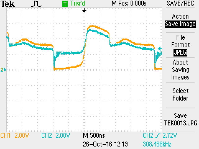
Yellow is the collector of Q2 and the blue is the base of Q1.

Very interesting waveshape.  Let’s see how this circuit works.

When power is applied, Q1 and Q2 turn on.  Collector of Q2 pulls to ground.  Since current cannot change instantaneously, the voltage applied across the inductor allows a fixed di/dt to charge the inductor, L1.  The current starts flowing in a roughly linear fashion until the maximum current that can be supplied by Q2 is reached…at which time di/dt falls to zero.

analysis1

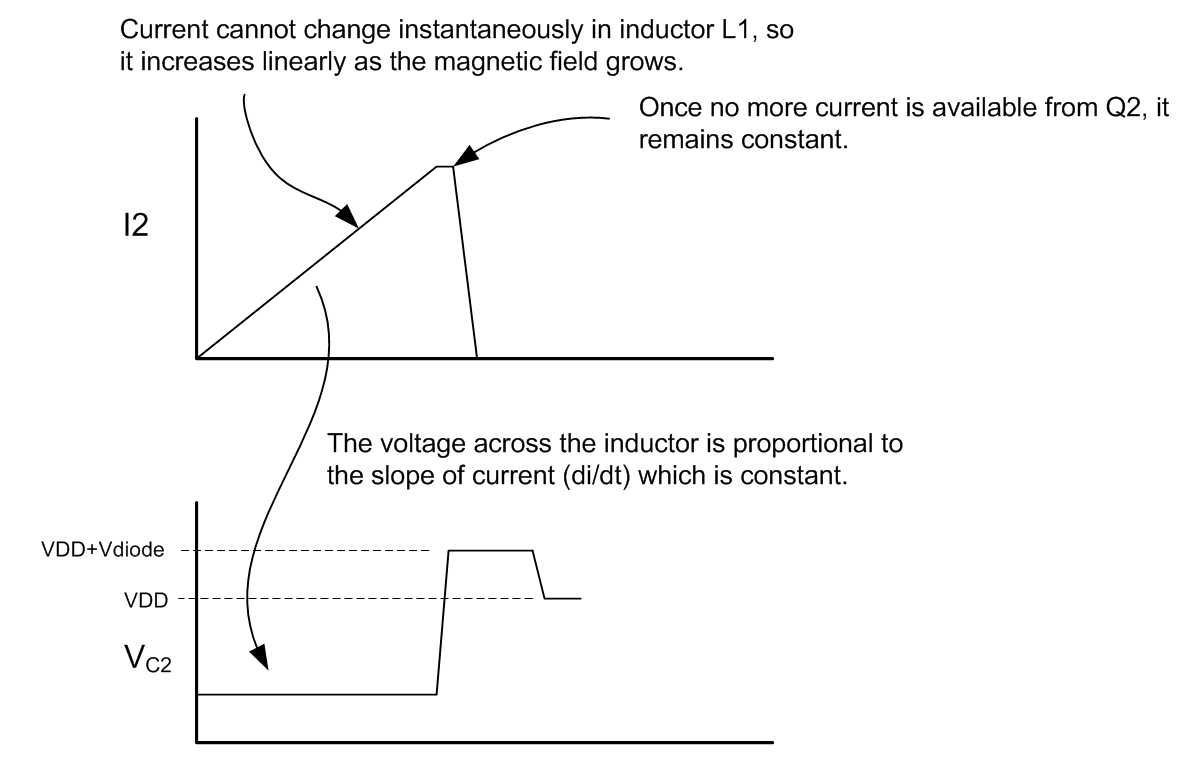
When Q2 current saturates, di/dt=0 and the inductor cannot maintain the voltage across it so the collector of Q2 swings positive.   This voltage couples to the base of Q1 to turn it off  (positive feedback) and thereby cutting off the Q2 collector current to the inductor which tries to maintain its magnetic field and propels even more positive until it discharges through the diode.

analysis2

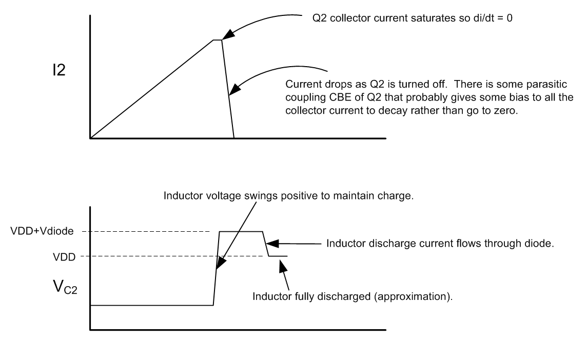
Inductor discharge current flows through diode until the voltage collapses across the inductor.  The time in this state is determined by the R1*C1 time constant.  By modifying this time constant, this pedestal can be lengthened or shortened.

The inductor cannot completely discharge through the diode because of the diode junction voltage requirement.  The inductor must finish discharging via parasitic paths in the circuit.  The only path for discharge is through C1 and CBE in parallel with R1 as shown below.

ringing

The inductor discharges via the parasitic path until the base of Q1 discharges enough to turn on Q1 and repeat the cycle.

A simulation of the circuit illustrates the phases of operation.

lcsimulation

If the RC time constant is chosen short enough, the portion of the waveform that is ringing can be eliminated.

OK…interesting circuit.  Quite complicated due to the inductor.  It does oscillate.  But why would you build such a circuit.  Well, perhaps for the LED drive. Typically, and LED may require a forward voltage of 1.8 to 2.8 volts.  If you wanted to power the oscillator with a single cell, then maybe you need the inductor kick-back voltage for that.

9-Axis Motion Sensor

A client asked me to develop a multi-axis sensor for embedded applications.  It needed a gyro, accellerometer, and a magnetometer, so I decided on the Invensis 9150 9-axis motion sensor.  In order to output the data to something, I used Bluetooth LE so that I could communicate with a smart phone (Android or IOS).  At the time, the most popular BTLE device seemed to be the Nordic nRF8001.  For control, I could have gone several ways.  There was a lot of code in the public domain using Arduino which is based on Atmel AVR devices primarily.  However, due to my roots, I decided on the Silicon Labs C8051F931.  The circuit design was easy.  Most of the work had already been done by others in terms of the radio…the rest was just connecting pins!  Here is the schematic.

Board schematic

Next task was to do the board layout.  I have a guy that is good at this sort of thing, so I contracted it out…both board design and assembly.  Here is the result.

Board

Once the schematic was done, I set about writing the code.  I started with the codebase that was developed for the Arduino.  Basically, I had to port everything over to the Silabs MCU.  It was not trivial, but after some effort, I got it working.

I also benefited from the work Nordic and others had done on the smartphone side.  So I had my son take the Arduino Android code and modify it to interface with my board.  Here is a screen shot of an Android phone showing the results being read from the board over BTLE.

screen

This was a great project!!

Wrap it up…

A long time ago, IC designers would breadboard their designs prior to committing to the fab.  This worked pretty well for small logic designs because MSI Logic was readily available (74xx series dominated) and the number of gates were generally manageable.  We used panels of wire-wrap sockets for the designs and they were wired using wire-wrap.  Wire-wrap was a 30-gauge wire with a thin Teflon coating.  When wrapped tightly on a square gold-plated pin, the sharp edges of the pin cut through the Teflon coating, making a connection.

Noting is perfect.  Sometimes the wrap was not tight enough to make a secure electrical contact.  Sometimes, a connection was simply missed.  Rather than installing the chips and troubleshooting with oscilloscopes and logic analyzers, the breadboard was first tested for continuity…every connection on the schematic was verified.  This was a tedious process.

A common tool for this job was a “buzz box” or continuity checker, as it were.  Rather than register a visual reading, an audible “buzz” indicated a good connection.

I had the idea for a “buzz box” back in 1981.  The idea was motivated by several things.  First, I did not want to have a power switch because invariably, the thing would be left on and the battery run down.  Second, I wanted the ability to buzz out circuits where chips were installed.  These were two interesting challenges.

The idea I am presenting here came to me one morning as I awoke–I had been pondering this day and night.  I immediately sketched out the idea on a piece of paper and when I got to the office, I set about proving the concept.  It worked…it was beautiful.  I thought it to be so clever that I submitted it to a publication “Electronics” for an article in their “Designer’s Notebook” section.  Sure enough the article was accepted and I got $50 for my trouble.

Here it is scanned from Nov 13, 1981 edition of Electronics.

Continuity Tester_schematic

Time flies like an arrow…

I was cleaning out my files last week and ran across this.  It is a kitchen timer I made for my mom a long time ago…I am guessing early 80s.  The thing that made me laugh was not the diode logic but that I labeled it “Timer for Mother.”  Why did I say “Mother” instead of “Mom?”  I call her “Mom” now and it feels like I have all ways called her that.  She is 97 and still mentally sharp.  She does not cook any longer so does not need the timer…I still have it though.

Kitchen Timer

Found when I wasn’t looking…

One of the things I do is read patents.  Few inventions jump out at me but now and then one leaps from the page.  Here is one that really caught my eye.  It is a circuit that performs a common function but in a different way.  I will let you figure it out!

2015-03-19 08_21_03-Current Mirror.vsd - Microsoft VisioIgnore body effect!